News Posts matching #Intel 14A

Return to Keyword Browsing

Siemens and Intel Foundry Collaborates on Integrated Circuits and Advanced Packaging Solutions for 2D and 3D IC

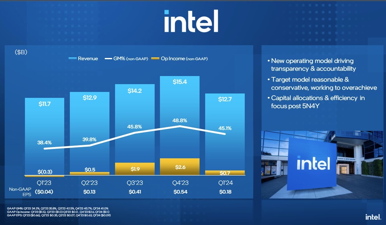
Siemens Digital Industries Software today announced that its continued collaboration with Intel Foundry has resulted in multiple product certifications, updated foundry reference flows, and additional technology enablement leveraging the foundry's leading-edge technologies for next-generation integrated circuits (IC) and advanced packaging. Siemens is a founding partner of the Intel Foundry Accelerator Chiplet Alliance - enabling a new and compelling solution for 3D IC and chiplet offerings to a breadth of semiconductor market verticals.

Intel 18A Certification Achievements
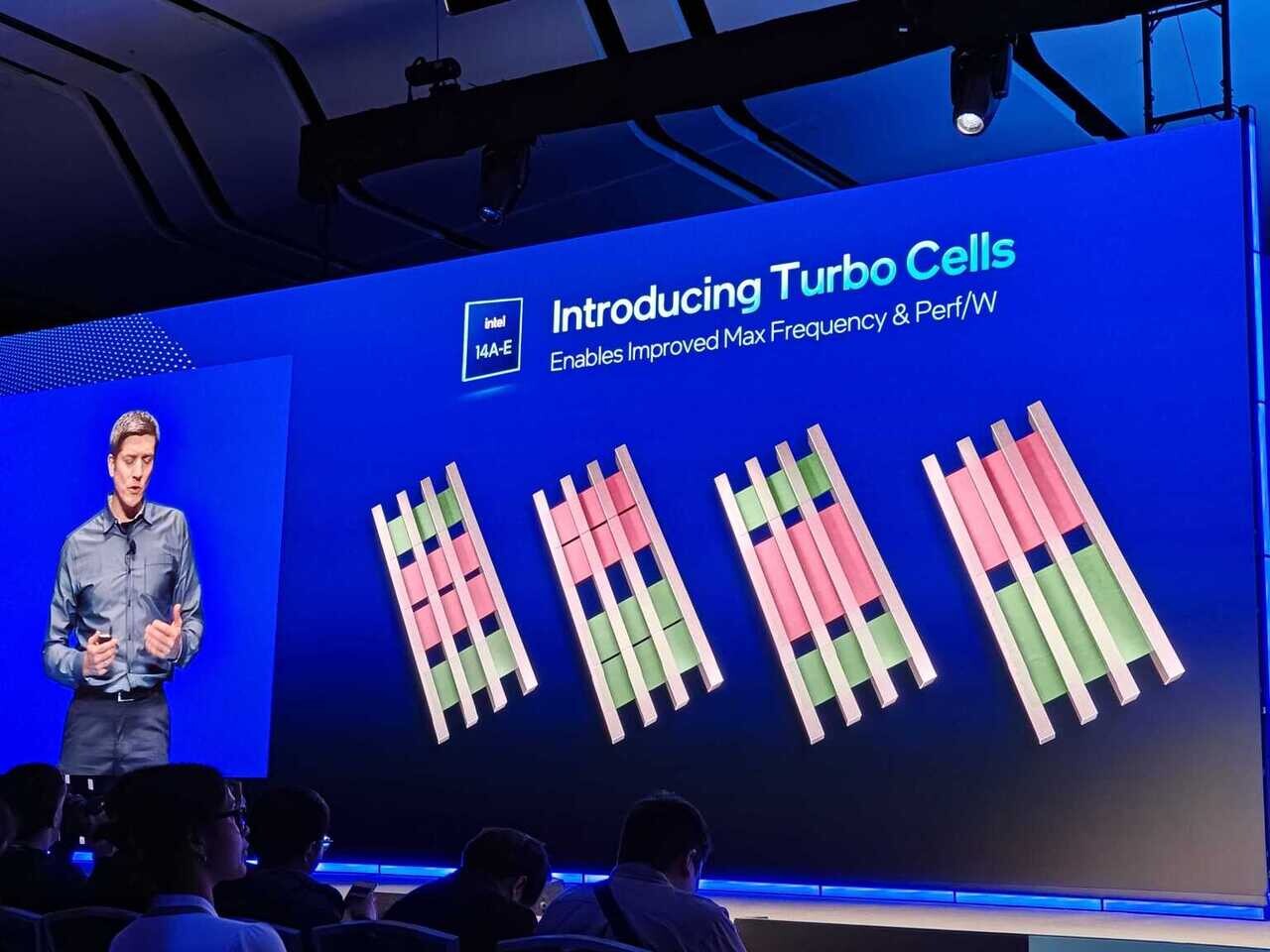
Siemens' industry-leading Calibre nmPlatform tool is now certified for the latest Intel 18A production Process Design Kit (PDK). Intel 18A represents a significant technological leap forward, featuring innovative RibbonFET Gate-all-around transistors and the industry's first PowerVia backside power delivery. This Calibre certification allows mutual customers to continue leveraging the Calibre nmPlatform tool as their industry-standard sign-off solution with Intel Foundry's most advanced manufacturing process, accelerating time-to-market for next-generation chip designs.

Intel 14A Node Debuts "Turbo Cells" to Boost Frequency and Cut Power

During Intel's Foundry Direct Connect symposium in San Jose, where Intel confirmed the ramp of the 18A node at the Arizona fab, the company also announced Intel has achieved a significant advancement in its future node development with the announcement of "turbo cell" technology for its upcoming 14A process. Now slated for production in 2027, this progress supports Intel's objective of introducing five process nodes within a four-year period. The 18A node is presently in risk production and incorporates RibbonFET gate-all-around transistors along with PowerVia, Intel's backside power-delivery architecture. Intel anticipates transitioning 18A to full-volume manufacturing later this year, thereby internalizing greater chiplet assembly work that was previously outsourced for designs such as Lunar Lake.

For the upcoming 14A process, it combines second-generation RibbonFET with PowerDirect, the company's enhanced power network. When implemented using High-NA EUV lithography, Intel projects a performance-per-watt gain of between 15 and 20 percent over the 18A process. Of particular interest is the introduction of turbo cells. These specialized standard-cell libraries enable designers to integrate both high-performance and energy-efficient cells within a single design block. Such flexibility permits precise optimization of chip speed, power consumption, and die area to meet diverse application requirements. In practical terms, turbo cells are expected to elevate peak CPU frequencies and accelerate critical GPU pathways without incurring substantial energy penalties. Intel has already distributed its PDK for the 14A node to prospective customers for feedback, with multiple partners already planning test-chip tape-outs. Complementing these advances, the company will employ advanced packaging technologies, including Foveros 3D stacking and EMIB, and a new high-bandwidth EMIB-T variant to integrate 14A and 18A dies within unified hybrid packages.

Intel Foundry Gathers Customers and Partners, Outlines Priorities

Today at Intel Foundry Direct Connect, the company will share progress on multiple generations of its core process and advanced packaging technologies. The company will also announce new ecosystem programs and partnerships, and welcome industry leaders to discuss how a systems foundry approach enables collaboration with partners and unlocks innovation for customers.

Intel CEO Lip-Bu Tan will open the event by discussing Intel Foundry's progress and priorities as the company drives the next phase of its foundry strategy. Naga Chandrasekaran, Intel Foundry chief technology and operations officer, and Kevin O'Buckley, general manager of Foundry Services, will also deliver keynotes during the morning session, sharing process and advanced packaging news while highlighting Intel Foundry's globally diverse manufacturing and supply chain.

High-NA EUV Tools Cost Nearly $400 Million Yet Deliver Big Savings on Complex Layers

High‑NA EUV lithography comes with a crazy $380 million price tag, but it can actually cut overall production costs in the right situations. At the SPIE Advanced Lithography and Patterning conference in February 2025, IBM researchers in Veldhoven revealed that one high‑NA exposure runs about 2.5x the cost of a standard low‑NA shot. That seems steep, yet High‑NA's real strength shows up when it replaces complicated multi‑patterning processes. SemiAnalysis had predicted last year that High‑NA would not become cost‑effective until around 2030, largely because higher dose requirements slow down throughput on the trickiest layers. However, after reviewing IBM's new data, the firm adjusted its outlook. Their model confirms that sticking with Low‑NA double patterning for two-mask sequences remains the cheapest path.

On the other hand, once you need three or more Low‑NA masks, switching to a single High‑NA pass starts to pay off. In fact, for a four‑mask self‑aligned litho‑etch flow, High‑NA can reduce total wafer cost by roughly 1.7-2.1x compared to using Low‑NA multi‑patterning. One big reason fabs are interested is that fewer exposures mean simpler process flows. You cut down cycle time and lower the chance of overlay mistakes. Still, SemiAnalysis warns that a simpler flow does not automatically mean lower expense in every case. Looking at Intel 14A, it turns out only a few critical metal layers at the 14A node hit the sweet spot where High‑NA's higher per‑shot cost is outweighed by ditching multiple masks.

Intel Completes Second ASML High-NA EUV Machine Installation

According to TechNews Taiwan, Intel has made significant progress in implementing ASML's cutting-edge High-NA EUV lithography technology. The company has successfully completed the assembly of its second High-NA "Twinscan EXE" EUV system at its Portland facility, as confirmed by Mark Phillips, Intel's Director of Lithography Hardware. Christophe Fouquet, CEO of ASML, highlighted that the new assembly process allows for direct installation at the customer's site, eliminating the need for disassembly and reassembly, thus saving time and resources. Phillips expressed enthusiasm about the technology, noting that the improvements offered by High-NA EUV machines have surpassed expectations compared to standard EUV systems. Given the massive $380 million price point of these High-NA systems, any savings are valuable in the process.

The rapid progress in installation and implementation of High-NA EUV technology at Intel's facilities positions the company strongly for production transition. With all necessary infrastructure in place and inspections of High-NA EUV masks already underway, Intel aims to have its Intel 14A process in mass production by 2026-2027. As Intel leads in High-NA EUV adoption, other industry giants are following suit. ASML plans to deliver High-NA EUV systems to TSMC by year-end, with rumors suggesting that TSMC's first system will possibly arrive in September. Samsung has also committed to the technology, although recent reports indicate a potential reduction in their procurement plans. Additionally, this development has sparked discussions about the future of photoresist technology, with Phillips suggesting that while Chemically Amplified Resist (CAR) is currently sufficient, future advancements may require metal oxide photoresists. This provides a small insight into Intel's future nodes.

Pat Gelsinger Writes to Employees on Foundry Momentum, Progress on Plan

All eyes have been on Intel since we announced Q2 earnings. There has been no shortage of rumors and speculation about the company, including last week's Board of Directors meeting, so I'm writing today to provide some updates and outline what comes next. Let me start by saying we had a highly productive and supportive Board meeting. We have a strong Board comprised of independent directors whose job it is to challenge and push us to perform at our best. And we had deep discussions about our strategy, our portfolio and the immediate progress we are making against the plan we announced on August 1.

The Board and I agreed that we have a lot of work ahead to drive greater efficiency, improve our profitability and enhance our market competitiveness—and there are three key takeaways from last week's meeting that I want to focus on:
  • We must build on our momentum in Foundry as we near the launch of Intel 18A and drive greater capital efficiency across this part of our business.
  • We must continue acting with urgency to create a more competitive cost structure and deliver the $10B in savings target we announced last month.
  • We must refocus on our strong x86 franchise as we drive our AI strategy while streamlining our product portfolio in service to Intel customers and partners.
We have several pieces of news to share that support these priorities.

Intel Reports First-Quarter 2024 Financial Results

Intel Corporation today reported first-quarter 2024 financial results. "We are making steady progress against our priorities and delivered a solid quarter," said Pat Gelsinger, Intel CEO. "Strong innovation across our client, edge and data center portfolios drove double-digit revenue growth in Intel Products. With Intel 3 in high-volume production, leading-edge semiconductors are being manufactured in the U.S. for the first time in almost a decade and we are on track to regain process leadership next year as we grow Intel Foundry. We are confident in our plans to drive sequential growth throughout the year as we accelerate our AI solutions and maintain our relentless focus on execution, operational discipline and shareholder value creation in a dynamic market."

"Q1 revenue was in line with our expectations, and we delivered non-GAAP EPS above our guidance, driven by better-than-expected gross margins and strong expense discipline," said David Zinsner, Intel CFO. "Our new foundry operating model, which provides greater transparency and accountability, is already driving better decision-making across the business. Looking ahead, we expect to deliver year-over-year revenue and non-GAAP EPS growth in fiscal year 2024, including roughly 200 basis points of full-year gross margin improvement." In the first quarter, the company used $1.2 billion in cash from operations and paid dividends of $0.5 billion.

Intel 10A (1 nm-class) Node to Enter Mass Production in 2027

Last week at the Intel Foundry Services Connect event, Intel unveiled its Intel 14A foundry node (1.4 nm-class), to succeed its Intel 18A and Intel 20A nodes, with mass production on this node expected to commence in 2026. It turns out that there is an even more advanced node Intel is working on, which it didn't announce last week, but which was part of an NDA presentation that the company forgot to lift. We're talking about the new Intel 10A node, a 1 nm-class silicon fabrication node that's a generation ahead of Intel 20A. The company says that it expects mass production on the node to begin toward the end of 2027. It is on the backs of these sub-2 nm class nodes, and the impending organizational changes that sees Intel Foundry Services become a more independent commercial entity, that Intel CEO Pat Gelsinger thinks that Intel will become the "TSMC of the West."

Currently, fabs that utilize EUV (extreme ultraviolet) lithography, namely the Intel 4, Intel 3, and Intel 20A; together make barely 15% of Intel's wafer volumes, with the bulk of the foundry's production focusing on the DUV based Intel 7. EUV-based nodes are expected to linearly grow till 2025, but what's interesting is that Intel doesn't see the kind of multi-year stagnation on Intel 4 and Intel 3 that it's currently experiencing with Intel 7; with wafer volumes of Intel 20A and 18A expected to exceed those of the Intel 4 and Intel 3 within 2025. By 2026, Intel expects that there will be twice as many Intel 20A/18A wafers pushed as Intel 4 and Intel 3. Although they use EUV, Intel 4 and Intel 3 are Intel's final nodes to implement FinFET transistors, as the company transitions to nanosheets with Intel 20A (which are called RibbonFETs in Intel jargon). Intel did not get into the technology behind Intel 10A. The company, along with Samsung and TSMC, demonstrated its stacked CFET transistor in 2023, which will power foundry nodes as nanosheets mature. Intel in its presentation also talked about the next wave of factory automation implemented by IFS, which sees AI-driven "cobots" (collaborative robots) replace humans for more roles in the clean room.

Intel Announces Intel 14A (1.4 nm) and Intel 3T Foundry Nodes, Launches World's First Systems Foundry Designed for the AI Era

Intel Corp. today launched Intel Foundry as a more sustainable systems foundry business designed for the AI era and announced an expanded process roadmap designed to establish leadership into the latter part of this decade. The company also highlighted customer momentum and support from ecosystem partners - including Synopsys, Cadence, Siemens and Ansys - who outlined their readiness to accelerate Intel Foundry customers' chip designs with tools, design flows and IP portfolios validated for Intel's advanced packaging and Intel 18A process technologies.

The announcements were made at Intel's first foundry event, Intel Foundry Direct Connect, where the company gathered customers, ecosystem companies and leaders from across the industry. Among the participants and speakers were U.S. Secretary of Commerce Gina Raimondo, Arm CEO Rene Haas, Microsoft CEO Satya Nadella, OpenAI CEO Sam Altman and others.
Return to Keyword Browsing
May 12th, 2025 11:17 +03 change timezone

New Forum Posts

Popular Reviews

Controversial News Posts

OSZAR »