News Posts matching #next-gen

Return to Keyword Browsing

Nintendo Will Contemplate Switch 2 Price Hikes - Dependent on Shifts in Tariff Conditions

Nintendo's Switch 2 hybrid console is set to arrive early next month (June 5), complete with promised launch prices. Early last month, the company's basic cost of entry for next-gen access—$450 (US)—seemed to be on tenuous ground. Nintendo and its retail partners decided to postpone their opening of pre-orders—affecting excited customers in the United States, then (days later) in Canada. Thanks to political posturing, a number of big industry players had to restrategize. Late last week, Microsoft announced their implementation of global Xbox Series price increases. In April, Sony revealed similar changes for PlayStation 5; restricted to select market territories. Nintendo has allowed a re-opening of Switch 2 pre-orders; gamers can secure core hardware at original MSRPs. Unfortunately, a compromise was made—first-party Switch 2 accessories will be more expensive, on launch day and beyond.

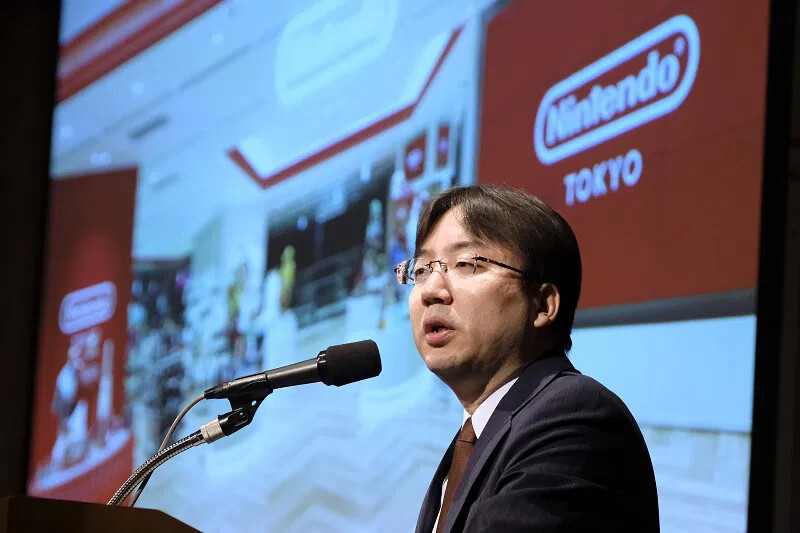
During a recent call with investors, Nintendo's president—Shuntaro Furukawa—confirmed that their core hardware pricing is subject to change. Launch price tags are safe (for the moment); the company will need to radiate some goodwill during their next-gen design's salad days. Commenting on a shifting political landscape, Furukawa-san stated: "at this time, the top priority is to quickly popularize the Switch 2 hardware...If the assumptions regarding tariffs change significantly, we would like to consider what price adjustments we should make, and implement them after considering various factors." Industry analysis has produced a scary projection; worst case scenarios could send tech prices up by roughly 70%. Considering the vintage of Switch 2's alleged internals, gaming hardware enthusiasts have questioned the value offered by this $450 hybrid handheld.

Insider Suggests "Snapdragon 8 Elite Gen 2" SoC NPU Computing Power Bumped Up to 100 TOPS

Digital Chat Station (DCS)—a dedicated watcher of futuristic smartphone chip developments—has returned to a favorite topic: Qualcomm's rumored "Snapdragon 8 Elite Gen 2" mobile chipset. The tenured technological soothsayer disclosed compelling "SM8850" details over a month ago; mostly focusing on key next-gen upgrades. His latest bulletin reiterates many past claims, but a new proposition points to a significant bump in onboard AI-crunching capabilities. DCS's latest dose of inside track knowledge points to the Gen 2 chip's NPU computing power being bumped up "to 100 TOPS."

At the tail end of their bulletin, DCS mentioned an interesting new feature: "(the SM8850) chip natively supports hardware-level sunlight screen; display brightness of new devices will be greatly improved, and the native-level super frame will be further improved." In a separate post, DCS hinted about a forthcoming "Snapdragon 8 flagship chip-powered" smartphone that will make use of a "new silicon" 7800 mAh capacity battery. Commenters have linked OnePlus to this development—Chinese electronics firms seem to be ahead of mainstream South Korean rivals, with their formulations of silicon-carbon battery technology. DCS's freshest theory did not place the cutting-edge "Snapdragon 8 Elite Gen 2" chip alongside a super high-capacity power cell, but examples of this potent combination could arrive later this year.

NEO Semiconductor Unveils Breakthrough 1T1C and 3T0C IGZO-Based 3D X-DRAM Technology

NEO Semiconductor, a leading developer of innovative technologies for 3D NAND flash memory and 3D DRAM, announced today the latest advancement in its groundbreaking 3D X-DRAM technology family—the industry-first 1T1C- and 3T0C-based 3D X-DRAM cell, a transformative solution designed to deliver unprecedented density, power efficiency, and scalability for the most demanding data applications.

Built on a 3D NAND-like architecture and with proof-of-concept test chips expected in 2026, the new 1T1C and 3T0C designs combine the performance of DRAM with the manufacturability of NAND, enabling cost-effective, high-yield production with densities up to 512 Gb—a 10x improvement over conventional DRAM.
"With the introduction of the 1T1C and 3T0C 3D X-DRAM, we are redefining what's possible in memory technology," said Andy Hsu, Founder & CEO of NEO Semiconductor. "This innovation pushes past the scaling limitations of today's DRAM and positions NEO as a frontrunner in next-generation memory."

TSMC Leadership Speaks of "Unprecedented" Demand for 2 nm; Greater Than Previous-gen Nodes

Despite recent whispers of TSMC losing a key 4 nm node process customer, industry analysts reckon that Taiwan's premier foundry business will remain in a comfortable leading position for the foreseeable future. "Optimistic" expert opinion points to "revenue growth for supply chain players," driven by the rapid progress of the firm's 2 nm manufacturing prowess. Naturally, their cutting-edge manufacturing capabilities—supposedly bolstered by GAAFET—are being tracked with keen interest. According to a fairly fresh Ctee Taiwan news piece, the usual big players are reportedly queued up and present within factory order books. The likes of Apple, NVIDIA, AMD, Qualcomm, MediaTek and Broadcom are mentioned. Mid-way through last month, Team Red officially announced a big collaborative milestone: "(our) next-generation AMD EPYC processor—codenamed "Venice"—is the first HPC product in the industry to be taped out and brought up on the TSMC advanced 2 nm (N2) process technology."

Ctee's report cites recent statements by C. C. Wei. Apparently, the TSMC CEO has stressed (on multiple occasions) that there is "unprecedented" demand for his company's 2 nm production pipelines—far exceeding previous levels for 3 nm. In addition, TSMC reps—who are currently touring the States; hosting technology symposiums—have revealed 2 nm (N2) defect density trends. Ctee outlined these intriguing details: "(N2's) defect density (D0) performance is comparable to that of the 5 nm family, and even surpasses the 7 nm and 3 nm processes of the same period, making it one of the most technologically mature advanced nodes." Wei's foundry team seems to be well ahead of main competition; insiders reckon that alleged equipment upgrades signal a push into 1.4 nm territories. Crucially, mass production of 2 nm (N2) wafers is expected to begin later this year—a cross-facility push was uttered by industry moles.

AMD Patents Provide Early UDNA Insights - "Blackwell-esque" Ray Tracing Performance Could be Achievable

Last September, AMD leadership publicly revealed UDNA—an "unforking" of previously separate enterprise and commercial GPU branches. Not long after this announcement, TechPowerUp's resident Serbian correspondent—AleksandarK—sat down with Team Red's Andrej Zdravkovic. The Chief Software Officer (and SVP) stated that a fair chunk of UDNA-related development work would be done by local engineers. Zdravkovic discussed this technology's eventual deployment in futuristic "AI PCs," but gamers have been salivating at the prospect of a proper successor to RDNA 4. A next-gen graphics architecture seeker—MrMPFR—has combed through official documents for any sign of UDNA preview material. The noted /Hardware subreddit member managed to distill their initial (very long) set of findings into an "easily digestible overview." They stated that this was just a small case of: "reporting and a little analysis on AMD's publicly available US patents filings," and other public-facing resources/archives.

Gleaned information included: "finalized architectural characteristics in future RDNA generations, AMD DXR IHV stacks (driver agnostic), and AMD sponsored titles. But please take everything with a grain of salt given my lack of professional expertise and experience with Real-time ray tracing (RTRT)". MrMPFR believes that Team Red started picking up former NVIDIA and Intel engineering talent, back in 2022/2023. In addition, a lot of new hires were apparently sourced from academic institutions. In theory, these newer team members have not had the time to make major inroads—in terms of getting finalized products out into the wild. MrMPFR reckons that noticeable contributions will accelerate AMD's making of "RDNA 6+/UDNA 2+," and beyond. Early 2025 leaks have pointed to the company collaborating with Sony; their "PlayStation 6" console is tipped to be powered by some fork of Team Red's "UDNA" graphics technology.

IBM Announces Granite 4.0 Tiny Preview - an Extremely Compact & Compute Efficient AI Model

We're excited to present IBM Granite 4.0 Tiny Preview, a preliminary version of the smallest model in the upcoming Granite 4.0 family of language models, to the open source community. Granite 4.0 Tiny Preview is extremely compact and compute efficient: at FP8 precision, several concurrent sessions performing long context (128K) tasks can be run on consumer grade hardware, including GPUs commonly available for under $350 USD. Though the model is only partially trained—it has only seen 2.5T of a planned 15T or more training tokens—it already offers performance rivaling that of IBM Granite 3.3 2B Instruct despite fewer active parameters and a roughly 72% reduction in memory requirements. We anticipate Granite 4.0 Tiny's performance to be on par with that of Granite 3.3 8B Instruct by the time it has completed training and post-training.

As its name suggests, Granite 4.0 Tiny will be among the smallest offerings in the Granite 4.0 model family. It will be officially released this summer as part of a model lineup that also includes Granite 4.0 Small and Granite 4.0 Medium. Granite 4.0 continues IBM's firm commitment to making efficiency and practicality the cornerstone of its enterprise LLM development. This preliminary version of Granite 4.0 Tiny is now available on Hugging Face—though we do not yet recommend the preview version for enterprise use—under a standard Apache 2.0 license. Our intent is to allow even GPU-poor developers to experiment and tinker with the model on consumer-grade GPUs. The model's novel architecture is pending support in Hugging Face transformers and vLLM, which we anticipate will be completed shortly for both projects. Official support to run this model locally through platform partners including Ollama and LMStudio is expected in time for the full model release later this summer.

"Official" AMD Ryzen Threadripper PRO "Shimada Peak" CPU Category Found by Data Miner

Mid-week, leakers produced an impressive list of unannounced next-gen AMD processor families—spanning across workstation, desktop, and laptop/notebook product lines. Additional data mining activities have outlined a possible "PRO model-only" release of Ryzen Threadripper Pro "Shimada Peak" 9000WX CPUs. AMD's upcoming Computex 2025 presentation plans could include an unveiling of their much-leaked Zen 5 workstation-grade processor family. Curiously, AMD's Technical Information Portal does not list a "Shimada Peak" High-End Desktop (HEDT) category—industry watchers expected to see a successor to the current-gen Ryzen Threadripper (non-PRO) 7000X "Storm Peak" series. In theory, next-gen HEDT models could be introduced at a later date. All leaked identifiers have featured "-5WX" affixes; denoting workstation deployments. Keen observers have not found products IPs ending with "-0X." InstLatX64's supplementary investigations seemed to confirm presences of the vast majority of recently disclosed next-wave product ranges—namely Ryzen 9000G "Gorgon Point" APUs and EPYC 4005 "Grado" CPUs. Another anomaly was discovered; the alleged Arm-based "Soundwave" SoC family was notably absent from Team Red's tech info repository.

Samsung "Exynos 2500" Variant Tipped as SoC of Choice for "Galaxy Z Flip 7"

Yesterday, Chosun Daily published a news report that alleges a key "Galaxy Z Flip 7-related" decision made by Samsung leadership. According to smartphone industry moles, the oft-leaked/rumored "Exynos 2500" chipset destined to debut in the company's next-gen (horizontal) foldable smartphone design. As stated in the South Korean insider article: "this is the first time that Samsung's own mobile application processor (AP) is being installed in a foldable phone." Prior to 2025, Galaxy Flip Z product lines made use of Qualcomm Snapdragon chipsets. Throughout early 2025, leaks have linked the "troubled" Exynos 2500 mobile processor to futuristic Galaxy Z Flip 7, Fold 7, and affordable "FE" Enterprise Edition models. The emergence of a superior 2 nm "Exynos 2600" flagship chip—apparently tailored for Galaxy S26 devices (2026)—has allegedly relegated the lesser SoC into lower leagues.

Semiconductor industry watchdogs reckon that the "Exynos 2500" will be manufactured via Samsung Foundry's own 3 nm GAA node process (aka SF3). Notebookcheck commented on this odd choice: "industry estimates from earlier suggested (SF3) yields were around 40%, making it less than ideal for mass production. But it seems Samsung decided to proceed anyway to save on costs, and likely give a new lease of life to its struggling foundry business." Jukanlosreve followed up with additional inside knowledge, just after the publication of Chosun Daily's news piece. The keen tracker of foundry-related revelations let slip with this observation: "the Exynos 2500 being used in the Flip 7 is said to be a lower-clocked chip due to its low yield. So it might as well be called the E2500E." Samsung is expected to unveil its Galaxy Z Flip 7 smartphone family during an "Unpacked" July event. Experts believe that Foundry employees will accumulate useful experience from the mass production of 3 nm parts; thus leading to improved output of finalized 2 nm (SF2) production lines.

NVIDIA RTX PRO 6000 Blackwell Workstation Edition PCB Layout Leaked By Insider

Over the past weekend, members of the Chiphell discussion board started posting truly NDA-busting photo material—one example made headlines a few days ago. A fairly convincing list of next-gen NVIDIA RTX PRO Blackwell series graphics cards appeared online just over a month ago; only a smattering of physical specimens have emerged since then. As pointed out by interested Chiphellers, Leadtek Chinese language websites have started listing a small selection of upcoming "Blackwell" generation professional SKUs.

The previously leaked PCB design was linked to Leadtek/NVIDIA's "blower-style" RTX PRO 6000 Blackwell Max-Q Workstation Edition 96 GB model. A brave Chiphell forumite has shared shots of another alleged internal component; a shorter PCB design has come to light—in VideoCardz's expert opinion, this stubby unit is destined to be contained within the Leadtek-made (non-Max-Q) RTX PRO 6000 Blackwell Workstation Edition enclosure. Official Team Green promotional renders have already presented this darker alternative to existing Founders Edition gaming-oriented siblings. According to VideoCardz, Team Green's Professional Blackwell series review embargo is still in effect and official launch window information is still not a publicly-known quantity. The freshly leaked bare PCB seems to borrow design elements—namely a dual-sided GDDR7 memory module mounting setup—from NVIDIA's familiar GeForce RTX 5090 Founders Edition model.

Samsung Reportedly Courting HBM4 Supply Interest From Big Players

The vast majority of High Bandwidth Memory (HBM) new stories—so far, in 2025—have involved or alluded to new-generation SK hynix and Micron products. As mentioned in recently published Samsung Electronics Q1 financial papers, company engineers are still working on "upcoming enhanced HBM3E products." Late last month, a neighbor/main rival publicly showcased their groundbreaking HBM4 memory solution—indicating a market leading development position. Samsung has officially roadmapped a futuristic "sixth-generation" HBM4 technology, but their immediate focus seems to be a targeted sales expansion of incoming "enhanced HBM3E 12H" products. Previously, the firm's Memory Business has lost HBM3 ground—within AI GPU/accelerator market segments—to key competitors.

Industry insiders believe that company leadership will attempt to regain lost market shares in a post-2025 world. As reported by South Korean news outlets, Kim Jae-joon (VP of Samsung's memory department) stated—during a recent earnings call, with analysts—that his team is: "already collaborating with multiple customers on custom versions based on both HBM4 and the enhanced HBM4E." The initiation of commercial shipments is anticipated at some point in 2026, hinging on mass production starting by the second half of this year. The boss notified listeners about development "running on schedule." A Hankyung article alleges that Samsung HBM4 evaluation samples have been sent out to "NVIDIA, Broadcom, and Google." Wccftech posits a positive early outlook: "Samsung will use its own 4 nm process from the foundry division and utilize the 10 nm 6th-generation 1c DRAM, which is known as one of the highest-end in the market. On paper, (their) HBM4 solution will be on par with competing models (from SK hynix), but we will have to wait and see."

Leaks Suggest AMD AM5 Future Support for Ryzen 9000G "Gorgon Point" & EPYC 4005 "Grado" CPUs

PC hardware watchers continue to pore over official AMD repositories and adjacent databases, in the hopes of finding unannounced next-gen technologies. Olrak29 and InstLatX64 have presented their latest Team Red-related findings; apparently reaching across futuristic desktop, mobile, and workstation product families. As outlined and interpreted by VideoCardz, several of these next-gen branches are already somewhat "known" properties—namely AMD's allegedly Zen 5-based Ryzen Threadripper "Shimada Peak" 9000WX (workstation) processor series. Following almost two years of leaks, an official introduction is expected to happen during Computex 2025. The Ryzen 9000G "Gorgon Point" desktop (Zen 5 + RDNA 3.5) APU series has turned up again; now "fully" linked to the AM5 socket platform (not a big surprise). The two leakers have also uncovered another rumored AM5-bound product lineup—"Grado" chips could be based on existing "Granite Ridge" foundations, but elevated to commercial/enterprise levels. These speculated basic/entry-level "EPYC 4005" processors are floated as natural successors to currently available 4004 forebears (related to Ryzen 7000 "Raphael" architecture).

Olrak29 and InstLatX64 have also found multiple mysterious FP8 socket-related Ryzen AI Mobile SoCs. "Krackan2" could be a cheaper refresh of current "Krackan Point" APUs—Tom's Hardware proposes smaller designs that sport fewer cores, and not configured with NPUs. Kepler_L2 has weighed in on the matter of three listed "Gorgon Point" IPs—he reckons that the third variant ("Gorgon Point3") will be a spin-off (aka refresh) of a "Krackan2" design. As suggested by insider knowledge, Team Red's convoluted scheme points to "Gorgon Point" being the sequel to "Strix Point." An FF5-based "Soundwave" processor design has appeared alongside the aforementioned futuristic Ryzen AI Mobile chipsets—industry whispers propose that AMD will be leveraging Arm architecture within a lower product tier. InstLatX64 pulled additional compelling information from AMD's Technical Information Portal—providing further insight into Ryzen AI "Medusa Point" APUs (Zen 6 + RDNA 3.5) being dreamt up, with a matching "larger footprint" FP10 platform.

Apple "Vision Air" Mixed Reality Headset Tipped for Late 2025/Early 2026 Launch

A series of April leaks have suggested that Apple's mixed reality headset engineering team is concocting two distinct next-gen solutions. Mid-month, leakers shared alleged early shots of "Vision Air"-related connectors and external parts—hinting at a potential dark blue colorway. Combined with a selection of fairly legitimate-sounding predictions from a notorious industry watcher, so-called Vision Pro sequels are on the way. Apple's Chinese manufacturing partners are reportedly deep into mass production of crucial "Vision Pro 2" components. Mark Gurman's "Power On" newsletter has provided plenty of inside knowledge stories over the past couple of months—his latest article included a section dedicated to fresh VR/AR insights: "I reported earlier this month that Apple is full steam ahead on two new successors to the Vision Pro (2023): a lighter version at a cheaper price point, and a Mac-tethered model aimed at applications that need maximum responsiveness."

He continued: "all signs point to the lighter model arriving between the end of this year and the first half of 2026. Despite the first version selling poorly, the company isn't abandoning ship here. The main uncertainty is whether the lighter version will be considered a replacement for the Vision Pro or a cheaper alternative." In theory, Apple could test "more mainstream" gaming waters with an initial rollout of the claimed cheaper + lightweight "Vision Air" model—perhaps set to do battle with readily available rival devices; e.g. Meta's dominant Quest 3 range. A full-blown Vision Pro follow-up could launch later on in 2026—likely reserved for upper-crust customers, with an increased focus on productivity applications.

TSMC Outlines Roadmap for Wafer-Scale Packaging and Bigger AI Packages

At this year's Technology Symposium, TSMC unveiled an engaging multi-year roadmap for its packaging technologies. TSMC's strategy splits into two main categories: Advanced Packaging and System-on-Wafer. Back in 2016, CoWoS-S debuted with four HBM stacks paired to N16 compute dies on a 1.5× reticle-limited interposer, which was an impressive feat at the time. Fast forward to 2025, and CoWoS-S now routinely supports eight HBM chips alongside N5 and N4 compute tiles within a 3.3× reticle budget. Its successor, CoWoS-R, increases interconnect bandwidth and brings N3-node compatibility without changing that reticle constraint. Looking toward 2027, TSMC will launch CoWoS-L. First up are large N3-node chiplets, followed by N2-node tiles, multiple I/O dies, and up to a dozen HBM3E or HBM4 stacks—all housed within a 5.5× reticle ceiling. It's hard to believe that eight HBM stacks once sounded ambitious—now they're just the starting point for next-gen AI accelerators inspired by AMD's Instinct MI450X and NVIDIA's Vera Rubin.

Integrated Fan-Out, or InFO, adds another dimension with flexible 3D assemblies. The original InFO bridge is already powering AMD's Instinct cards. Later this year, InFO-POP (package-on-package) and InFO-2.5D arrive, promising even denser chip stacking and unlocking new scaling potential on a single package, away from the 2D and 2.5D packaging we were used to, going into the third dimension. On the wafer scale, TSMC's System-on-Wafer lineup—SoW-P and SoW-X—has grown from specialized AI engines into a comprehensive roadmap mirroring logic-node progress. This year marks the first SoIC stacks from N3 to N4, with each tile up to 830 mm² and no hard limit on top-die size. That trajectory points to massive, ultra-dense packages, which is exactly what HPC and AI data centers will demand in the coming years.

Oracle Cloud Infrastructure Bolstered by Thousands of NVIDIA Blackwell GPUs

Oracle has stood up and optimized its first wave of liquid-cooled NVIDIA GB200 NVL72 racks in its data centers. Thousands of NVIDIA Blackwell GPUs are now being deployed and ready for customer use on NVIDIA DGX Cloud and Oracle Cloud Infrastructure (OCI) to develop and run next-generation reasoning models and AI agents. Oracle's state-of-the-art GB200 deployment includes high-speed NVIDIA Quantum-2 InfiniBand and NVIDIA Spectrum-X Ethernet networking to enable scalable, low-latency performance, as well as a full stack of software and database integrations from NVIDIA and OCI.

OCI, one of the world's largest and fastest-growing cloud service providers, is among the first to deploy NVIDIA GB200 NVL72 systems. The company has ambitious plans to build one of the world's largest Blackwell clusters. OCI Superclusters will scale beyond 100,000 NVIDIA Blackwell GPUs to meet the world's skyrocketing need for inference tokens and accelerated computing. The torrid pace of AI innovation continues as several companies including OpenAI have released new reasoning models in the past few weeks.

OKI Develops 124-Layer PCB Technology for Next-Generation Semiconductor Testing Equipment

OKI Circuit Technology, the OKI Group printed circuit board (PCB) company, has successfully developed 124-layer PCB technology for wafer inspection equipment designed for next-generation high bandwidth memory, such as HBM mounted on AI semiconductors. This is a roughly 15% increase in the number of layers over conventional 108-layer designs. OTC is seeking to establish mass production technology by October 2025 at its Joetsu Plant in Joetsu City, Niigata Prefecture, which has a proven track record and advanced development and production capabilities in the field of high multilayer, high-precision, large-format PCBs for semiconductor inspection equipment.

AI processing requires the transmission of vast data volumes between graphics processing unit (GPU) semiconductors and memory. As semiconductor performance increases, the memory installed is also required to have high-speed, high-frequency, and high-density data transfer capabilities. HBM features a stacked DRAM structure, requiring technology capable of fabricating wafers even more thinly and precisely. This configuration also requires that the PCBs used in inspection equipment meet even higher levels of performance and quality.

MSI Presenting AI's Next Leap at Japan IT Week Spring 2025

MSI, a leading global provider of high-performance server solutions, is bringing AI-driven innovation to Japan IT Week Spring 2025 at Booth #21-2 with high-performance server platforms built for next-generation AI and cloud computing workloads. MSI's NVIDIA MGX AI Servers deliver modular GPU-accelerated computing to optimize AI training and inference, while the Core Compute line of Multi-Node Servers maximize compute density and efficiency for AI inference and cloud service provider workloads. MSI's Open Compute line of ORv3 Servers enhance scalability and thermal efficiency in hyperscale AI deployments. MSI's Enterprise Servers provide balanced compute, storage, and networking for seamless AI workloads across cloud and edge. With deep expertise in system integration and AI-driven infrastructure, MSI is advancing the next generation of intelligent computing solutions to power AI's next leap.

"AI's advancement hinges on performance efficiency, compute density, and workload scalability. MSI's server platforms are engineered to accelerate model training, optimize inference, and maximize resource utilization—ensuring enterprises have the processing power to turn AI potential into real-world impact," said Danny Hsu, General Manager of MSI Enterprise Platform Solutions.

AMD Ryzen Threadripper "Shimada Peak" 9985WX 64-core CPU Discovered in Shipping Document

Going back to May 2023, an industry inside report suggested that AMD was planning a new generation Ryzen Threadripper High-End Desktop (HEDT) processor series. At the time, "Shimada Peak" was linked to a possible 2025 launch. Over the ensuing years, shipping manifests have revealed the transfer of various 9000 SKUs between Team Red facilities—starting with a mysterious 96-core prototype. Industry observers have been seeking out newer evidence of AMD's next-gen flagship "Zen 5" Threadripper chip; likely going under a "9995WX" moniker.

Late last week, a fresh leak unearthed a likely sub-flagship SKU: the 9985WX. This alleged 64-core SKU was spotted—by Everest (aka Olrak29)—alongside 9955WX (16-core) and 9945WX (12-core) siblings, in a shipping manifest. As reported on TechPowerUp on March 21, the same source uncovered two other entry-level models: the 9975WX (32-core) and 9965WX (24-core) parts. Unfortunately, Team Red's rumored monstrous 96-core 9995WX processor was not listed within fresh batches of shipping documents. Industry watchdogs expect AMD to repeat its product layout from past generations; spanning from entry-tier 12-core offerings up to the aforementioned 96-core range-topper. The latest leak suggests utilization of the SP6 socket type, and 350 W TDPs (across all product identifiers).

EK to Showcase Latest Liquid Cooling Innovations at Computex 2025

EK, renowned for its premium liquid cooling solutions and now managed by LM TEK, is set to present its latest innovations at COMPUTEX Taipei 2025. From May 20 to 23, attendees can visit LM TEK at Booth M1419, Hall 1 (4F), TaiNEX 1, to explore cutting-edge cooling technologies designed to meet the demands of next-generation AI computing. As artificial intelligence and high-performance computing continue to evolve, the need for efficient thermal management becomes increasingly critical. EK's newest solutions address these challenges head-on, offering advanced liquid cooling systems that elevate performance, ensure system stability, and meet the rigorous demands of modern AI workloads. This year's COMPUTEX will serve as a platform for EK to showcase how its innovative hardware—engineered for data centers, AI development platforms, and high-performance workstations—can help reshape the future of computing.

Want to know what's coming?
Visit our EK COMPUTEX 2025 page, where we will be revealing newly released products, exclusive launches, and spotlighting key partner projects on display at the show. Under the management of LM TEK, EK continues to push the boundaries of thermal management technology. This transition brings enhanced operational agility and a sharper focus on customer needs, while maintaining the trusted EK quality and design excellence. Visitors to the EK booth will have the opportunity to explore the latest liquid cooling solutions, meet the team, and discuss how EK technology can power next-gen AI innovation. Whether you're an industry professional, system integrator, or tech enthusiast, this is your chance to experience the future of liquid cooling—up close.

Sony Reportedly Prepping "PlayStation 6 Portable" with "<40 CU" Chipset Design

Sony and Microsoft seem to be involved in the development of handheld gaming consoles, but insiders reckon that respective next-generation offerings will not directly compete with each other. Xbox and ASUS have signalled some sort of collaborative ROG Alloy-esque device; potentially releasing later on in 2025. Whispers of a futuristic PlayStation portable model's chipset design emerged mid-way through March; courtesy of Kepler_L2. The notorious leaker has recent history of reporting inside track knowledge of AMD CPU and GPU architectures/technologies. They alleged that Sony and Team Red's collaborative PS6 APU design project had reached a finalized stage of development, possibly around late 2024/early 2025. Returning to March/April events; Kepler_L2 theorized that a "PS6 Portable" would not be capable of surpassing PlayStation 5 (home console) level performance upon launch in 2028.

The mysterious handheld is said to be powered by a "15 W SoC" manufactured on a non-specific 3 nm node process. Elaborating further, they posit that PlayStation's rumored handheld is capable of running PS5 generation games—bandwidth and power restrictions could reduce resolution and frame rates below that of Sony's current-gen system. Kepler_L2 pictures "PS6 Portable" gaming performance being somewhere in-between Xbox Series S and PlayStation 5 (non-Pro). According to rumors, the handheld's chipset is not related or derived from the PS6 home console's internal setup. Kepler_L2 envisioned a mobile SoC with fewer than 40 compute units (CUs)—several media outlets have added their interpretation of this data point; with a sub-36 count. PlayStation 5's GPU aspect consists of 36 CUs, while the Xbox Series S graphics solution makes do with 20 units. Sony's speculated return to portable territories will be welcomed by owners of older handheld models—namely the Vita and PSP. Famously, these portable products struggled to keep up with competing Nintendo devices.

ASUS ROG Crosshair X870E Extreme Motherboard Launching in China, Price Tag: ~$1360

Since teasing its next-gen flagship motherboard design—at CES 2025—the ASUS Republic of Gamers (ROG) team has spent time finalizing an option that is even more extravagant than their hardcore overclocking-oriented Crosshair X870E Apex model. Naturally, the premium sub-brand did not reveal pricing during preview events—instead, premature European e-tail listings suggested a €1200 (~$1350 USD) tag. Tony Wu and colleagues at ASUS China introduced an impressive swath of brand-new products at an official in-person showcase last week, in Changsha.

During proceedings, company representatives introduced their top-flight E-ATX format board with a hefty day one price: 9999 RMB ($1360 USD). The ASUS ROG Crosshair X870E Extreme is expected to launch later this month; likely starting off with the Chinese domestic market. At the time of writing, the manufacturer's various global branches have not disclosed localized details—be it pricing or availability. Last week's presser did not produce any surprises, since plenty of specification details (and promo shots) leaked out late last month. One interesting and very over the top feature is the model's integration of an adjustable full-color 5-inch LCD screen. The primary M.2 storage solution will be cooled by an "innovative" 3D vapor chamber heatsink. Well-heeled customers will be relieved to know that ASUS has outfitted the AAA board design with their revamped Q-Release Slim mechanism.

Apple "Vision Pro 2" Components Reportedly Being Mass Produced in China

Since its summer 2023 launch, Apple's pricey Vision Pro mixed reality headset has not exactly attracted a mainstream audience. Roughly a year later, rumors of a (then) recently canceled successor appeared online—insiders posited that company engineers had pivoted onto the development of a cheaper alternative model. Vision Pro "Version 1.0" arrived with an intimidating $3499 price tag; thus eliminating interest from a wide swath of potential AR/VR headset enthusiast customers. Industry insiders reckon that Apple had "abruptly reduced production" of the current-gen model last October, with further whispers suggesting a complete cessation of manufacturing activities by the end of 2024. Yesterday, an ITHome article cited compelling claims made by supply chain insiders—the initiation of mass production for a speculated second generation "Apple XR/Vision Pro" device.

The online report stated that: "multiple independent sources (have) confirmed that the panels, shells and other key components of the second-generation Apple XR headset are already in production." Very specific leaked information indicates Lens Technology being the exclusive supplier of glass panel pieces, and Changying Precision tasked with the making of the next-gen model's casing. Additionally, several contract circuit manufacturers are supposedly "rushing to complete orders." Secretive figures posit that Apple will release its sequel mixed reality headset later on in 2025. Differing "expert opinions" have not determined whether this incoming set of fancy goggles will be the predicted "cheaper" model, or a proper "M5 SoC-powered" successor.

Insider Report Suggests Start of 1 nm Chip Development at Samsung, Alleged 2029 Mass Production Phase Targeted

Samsung's foundry business seems to be busying itself with the rumored refinement of a 2 nm GAA (SF2) manufacturing node process—for possible mass production by the end of 2025, but company leadership will very likely be considering longer term goals. Mid-way through last month, industry moles posited that the megacorporation's semiconductor branch was questioning the future of a further out 1.4 nm (SF1.4) production line. Officially published roadmaps have this advanced technology rolling out by 2027. Despite present day "turmoil," insiders believe that a new team has been established—tasked with the creation of a so-called "dream semiconductor process." According to a fresh Sedaily news article, this fledgling department has started development of a 1 nm foundry process.

Anonymous sources claim that Samsung executives are keeping a watchful eye on a main competitor—as stated in the latest South Korean report: "there is a realistic gap with Taiwan's TSMC in technologies that are close to mass production, such as the 2 nm process, the company plans to speed up the development of the 1 nm process, a future technology, to create an opportunity for a turnaround." A portion of the alleged "1 nm development chip team" reportedly consists of veteran researchers from prior-gen projects. Semiconductor industry watchdogs theorize that a canceled SF1.4 line could be replaced by an even more advanced process. Sedaily outlined necessary hardware upgrades: "the 1.0 nanometer process requires a new technology concept that breaks the mold of existing designs as well as the introduction of next-generation equipment such as high-NA EUV exposure equipment. The company is targeting mass production after 2029." Samsung's current Advanced Technology Roadmap does not extend beyond 2027—inside sources claim that the decision to roll with 1.0 nm was made at some point last month.

Nintendo Confirms That Switch 2 Joy-Cons Will Not Utilize Hall Effect Stick Technology

Following last week's jam-packed Switch 2 presentation, Nintendo staffers engaged in conversation with media outlets. To the surprise of many, a high level member of the incoming console's design team was quite comfortable with his name-dropping of NVIDIA graphics technologies. Meanwhile, Team Green was tasked with the disclosing of Switch 2's "internal" workings. Attention has turned to the much anticipated-hybrid console's bundled-in detachable Joy-Cons—in the lead up to official unveilings, online debates swirled around potential next-gen controllers being upgraded with Hall Effect joystick modules. Many owners of first-gen Switch systems have expressed frustration regarding faulty Joy-Cons—eventually, Nintendo was coerced into offering free repairs for customers affected by dreaded "stick drift" issues. Unfortunately, it seems that the House of Mario has not opted to outfit its Gen 2.0 Joy-Cons with popular "anti-drift" tech.

As reported by Nintendo Life, Nate Bihldorff—senior vice president of product development and publishing at Nintendo of America—"outright confirmed the exclusion" of Hall Effect. Up until the publication of Nintendo Life's sit down interview, other company representatives have opined that Switch 2's default control system features very "durable feeling" sticks. When asked about the reason behind "new-gen modules (feeling) so different to the original Switch's analog stick," Bihldorff responded with: "well, the Joy-Con 2's controllers have been designed from the ground up. They're not Hall Effect sticks, but they feel really good. Did you experience both the Joy-Con and the Pro Controller?" The interviewer confirmed that they had prior experience with both new models. In response, Bihldorff continued: "so, I like both, but that Pro Controller, for some reason the first time I grabbed it, I was like, 'this feels like a GameCube controller.' I was a GameCube guy. Something about it felt so familiar, but the stick on that especially. I tried to spend a lot of time making sure that it was quiet. I don't know if you tried really whacking the stick around, but it really is (quiet)...(The Switch 2 Pro Controller) is one of the quietest controllers I've ever played." Nintendo will likely not discuss the "ins and outs" of its proprietary stick design, but inevitable independent teardowns of commercial hardware could verify the provenance of underlying mechanisms. Nowadays, hardcore game controller snobs prefer third-party solutions that sport Tunneling Magnetoresistance (TMR) joysticks.

Two Unannounced AMD Ryzen Z2 APU Models Leaked, Flagship Could be "AI Z2 Extreme"

Three months ago, AMD unveiled its Ryzen Z2 APU series at CES 2025—purpose made for deployment in next-gen handheld gaming PCs. The officially announced flagship—Ryzen Z2 Extreme "Strix Point," utilizing Zen 5 and RDNA 3.5 technologies—was previously alluded to by leakers in late 2024; albeit with some curious claims regarding an "odd 3+5 core configuration." Last week, Hoang Anh Phu (@AnhPhuH) presented an alleged expanded lineup of Ryzen Z2 processors—headlined by a mysterious "Ryzen AI Z2 Extreme" SKU.

PC hardware watchdogs believe that this speculative variant will eventually arrive with an enabled XDNA 2 NPU (a first for the series); likely readied to take on Intel's Core Ultra 200V "Lunar Lake" processor family. MSI's Core Ultra 7 258V-powered Claw 8 AI+ and Claw 7 AI+ handhelds launched not too long ago, boasting all sorts of Microsoft Copilot+ capabilities. Mid-way through March, an Xbox executive introduced "Copilot for Gaming." Team Red and manufacturing partners are likely jumping onto this "AI gaming" bandwagon with the aforementioned "AI Ryzen Z2 Extreme" chip, as well as Phu's fanciful "Ryzen Z2 A" model. The latter could be a spin-off of AMD's vanilla Ryzen Z2 "Hawk Point" design, with a "switched on" XDNA NPU.

China Develops HDMI Alternative: 192 Gbps Speeds and 480 W Power Delivery

A consortium of over 50 Chinese companies, including names like Huawei, Hisense, and TCL, has unveiled a domestic alternative to HDMI that offers up to 192 Gbps bandwidth and 480 W of power delivery. This new standard, the General Purpose Media Interface (GPMI), supports next-generation multimedia devices, meeting the growing demands of 8K resolution, higher refresh rates, and simplified connectivity. There are two variants available: a smaller Type-C model providing 96 Gbps and 240 W and a larger Type-B model delivering the full 192 Gbps and 480 W. Developed as a third-generation audio and video interface, GPMI addresses the limitations of older standards such as DVI and VGA while vastly outperforming HDMI 2.1's 48 Gbps and DisplayPort 2.1's 80 Gbps in data throughput. Its design enables bidirectional communication, seamlessly transmitting video, audio, data, and power over a single cable.

The standard's architecture includes a primary data link that can be split into various configurations—such as 6+2 or 1+7 channels—to adapt to different usage scenarios. In addition to its high-bandwidth data channels, GPMI features auxiliary links for device management, cable information, and a limited USB 2.0 connection. The Type-C variant, which has received approval from the USB Association, ensures compatibility with the USB-C ecosystem, helping with the integration for smart TVs and other connected devices. Primarily developed for the domestic market, GPMI also aims to reduce China's dependence on Western-controlled standards and licensing regimes.
Return to Keyword Browsing
May 11th, 2025 03:21 +03 change timezone

New Forum Posts

Popular Reviews

Controversial News Posts

OSZAR »